IIT Bombay · Founded Aug 2025 · India's First Student Chip Fab
India's first
student-built semiconductor fab
We build open-source semiconductor fabrication tools to make hands-on fabrication accessible
to students across India.
About Us
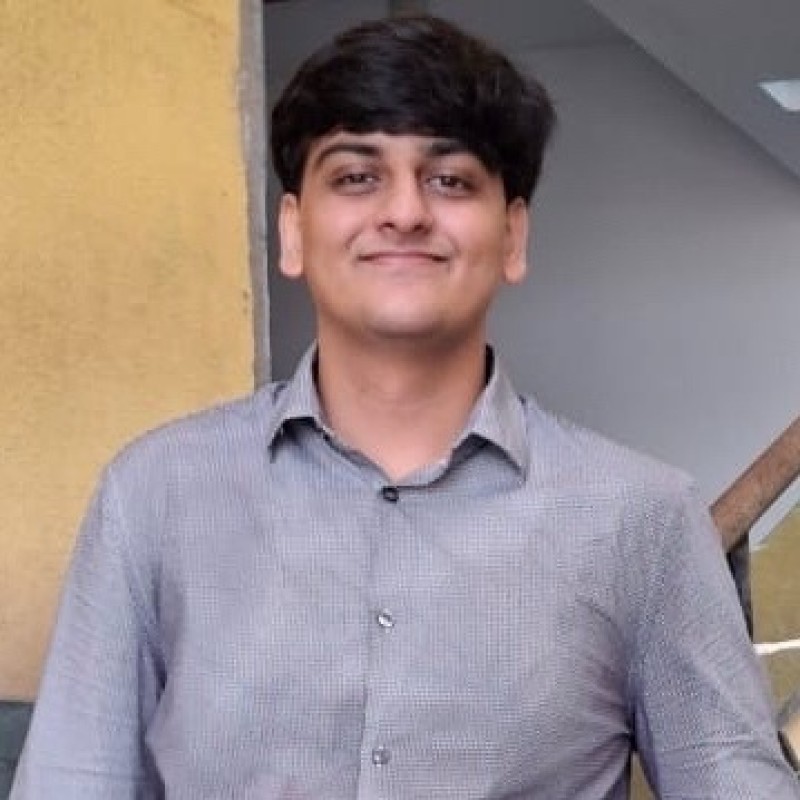
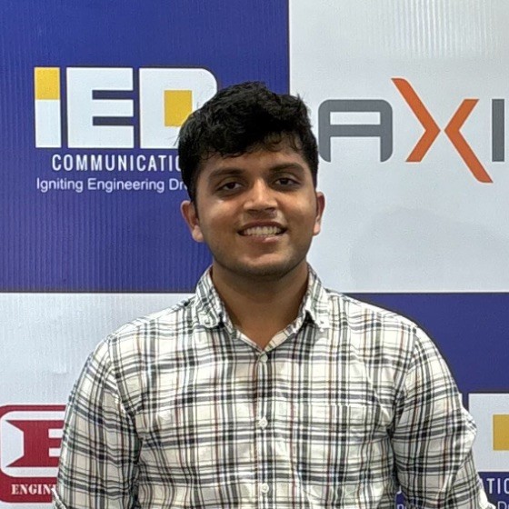
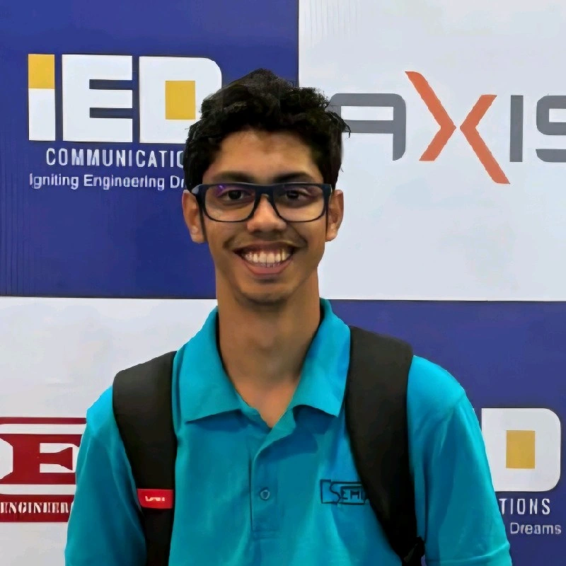
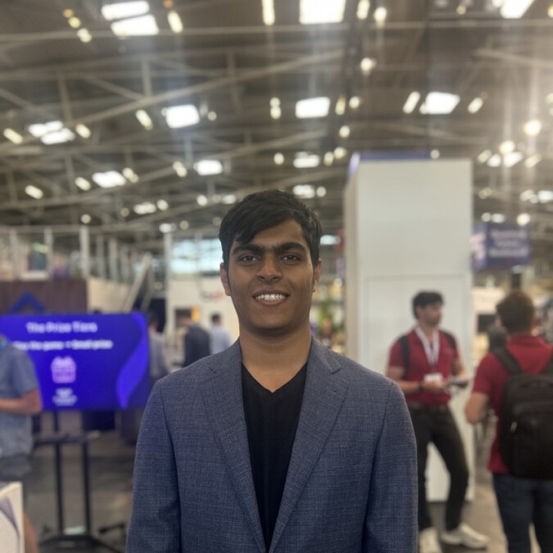
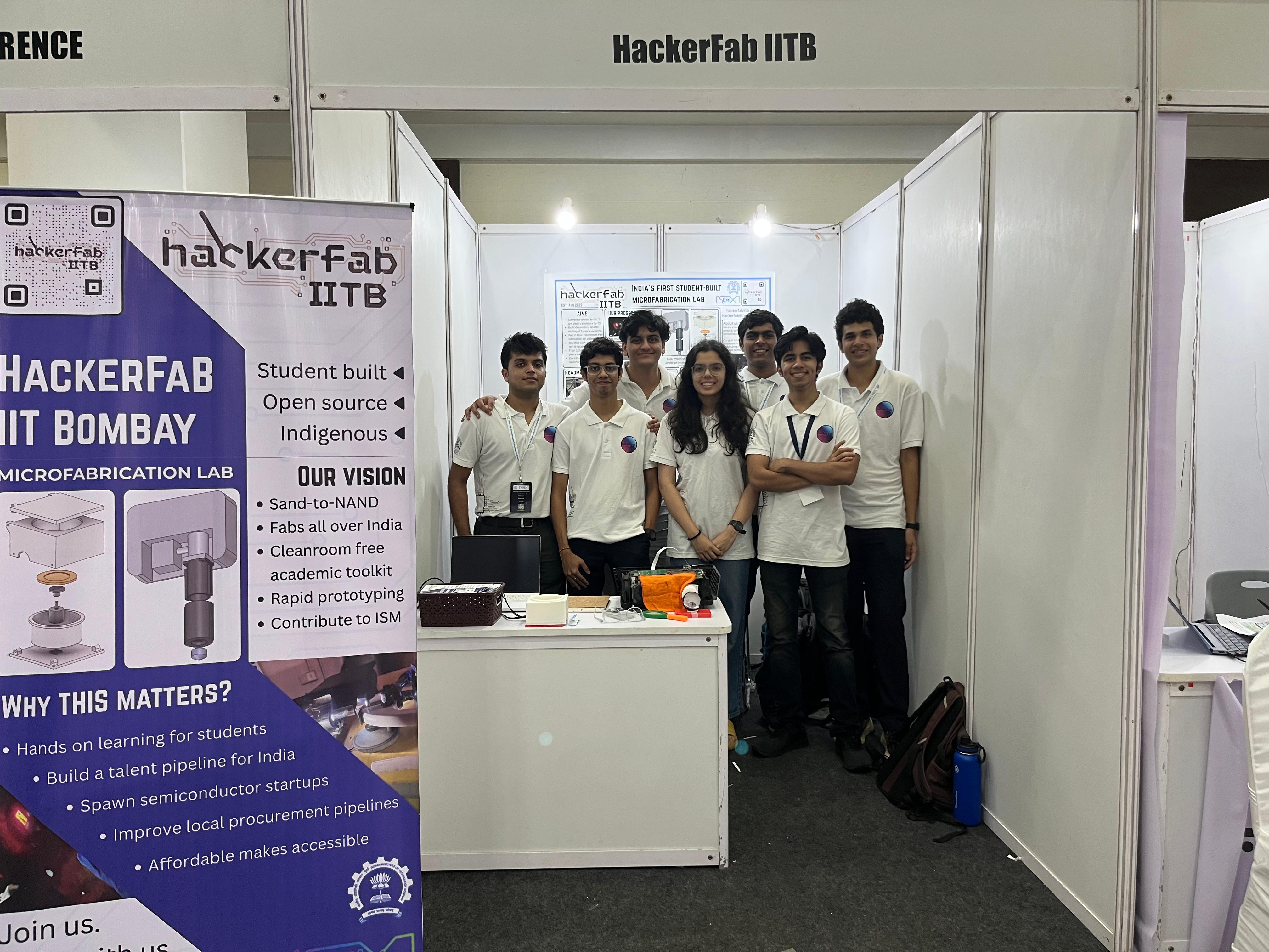
SemiX 2025
The HackerFab IITB team presenting to India's semiconductor community for the
first time.
click to flip
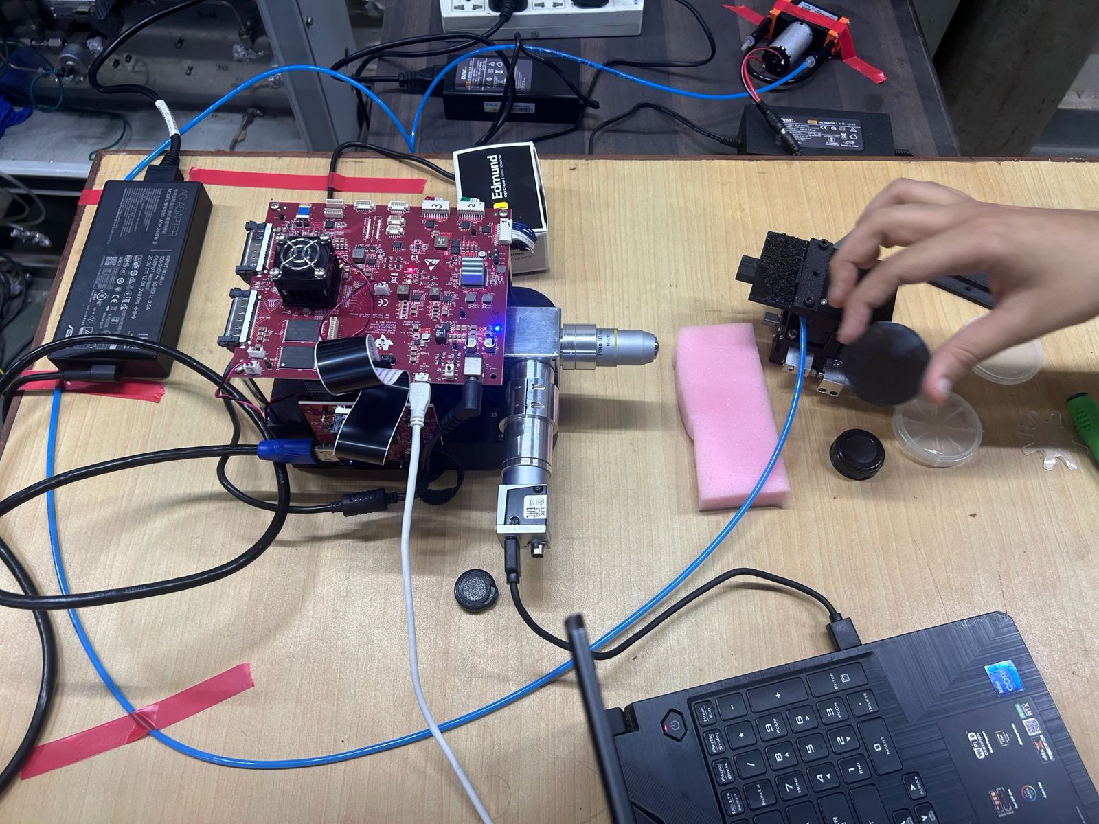
Maskless Lithography
1 µm feature size achieved on our home-built lithography system.
click to flip
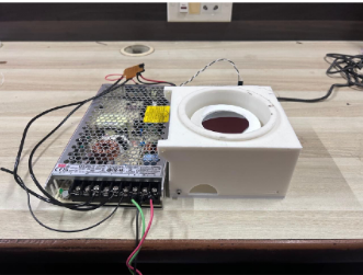
Spin Coater
Closed-loop control up to 6000 rpm. Fully student-built and open-source.
click to flip
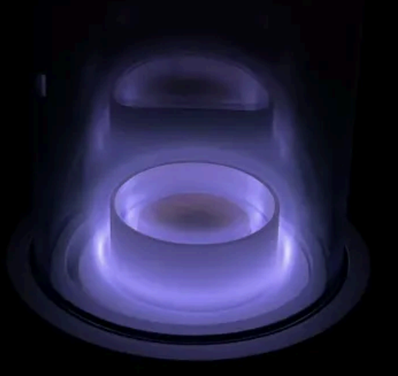
RF Sputtering
Our first deposition tool — thin film deposition coming soon.
click to flip
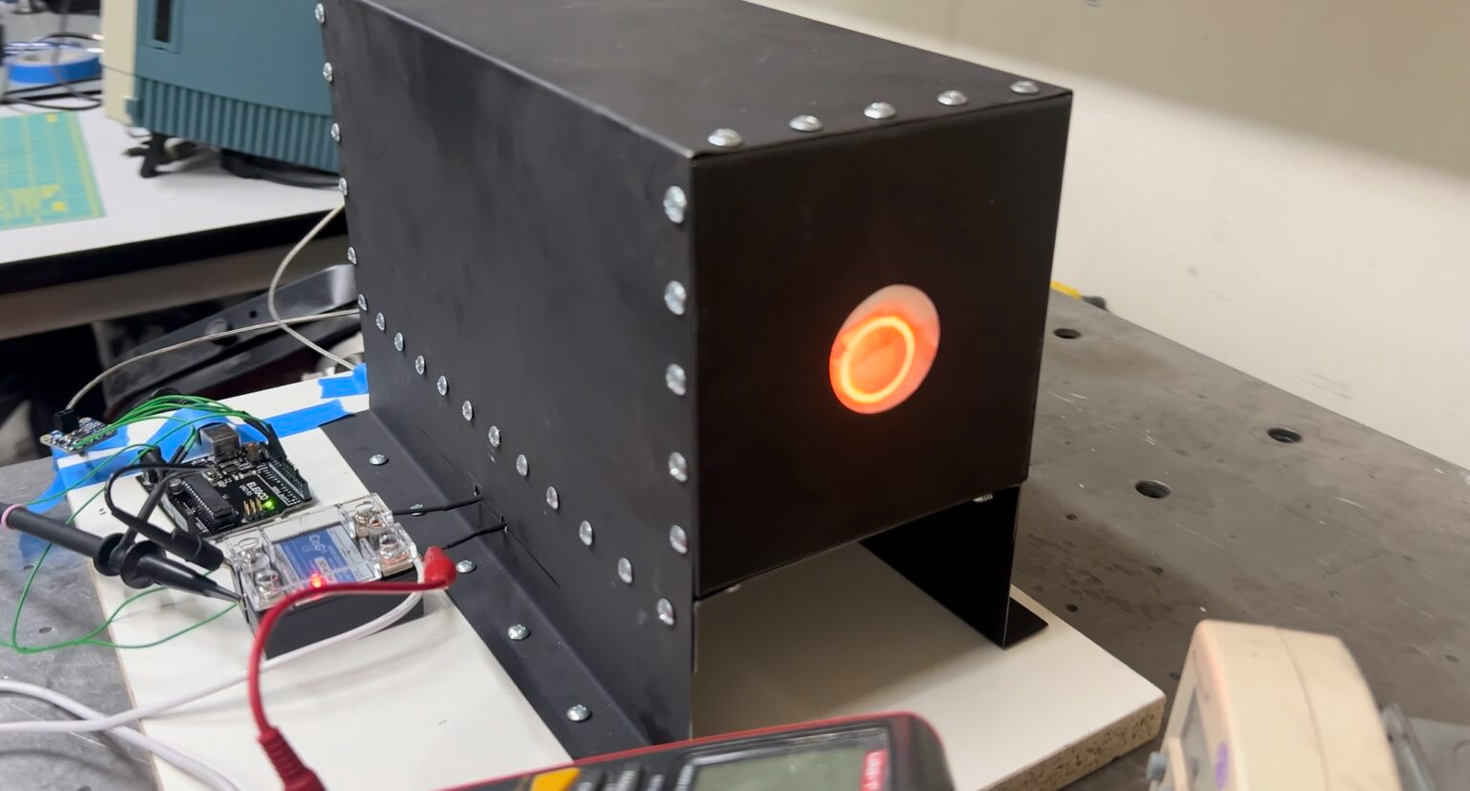
Tube Furnace
±2 °C precision up to 1100 °C for oxidation and
annealing.
click to flip
"Making hands-on chip fabrication accessible across India."
Founded in August 2025, we're a group of students determined to democratize technology and
foster innovation.
We are part of the
HackerFab network, aiming to become a stepping stone to the semiconductor industry.
Semiconductor Fabrication
Why should TSMC have all the fun?
Education
Integrating our tools with coursework at IITB
Open Source
Sharing tools, documentation and knowledge freely
Community
Join our Discord! Spreading this movement all over India
Our Goals
Technical Roadmap
Check out our journey so far, documentation and resources attached with each step.
In-Progress
Maskless Lithography
Achieved a pattern image of 1µm feature size.
In Progress
Spincoater
Demonstrated closed loop control up to 6000rpm
Planned
RF Sputtering
Our first deposition tool!
Planned
Tube Furnace
+/-2 degrees C at target temperatures up to 1100 degrees C
Growth & Outreach
Constantly trying to expand our community and bring HackerFab to more colleges across India.
Community Building
Growing our network of makers, students, and innovators across colleges in India. We
aim to establish chapters and partnerships with institutions nationwide.
Conferences & Talks
Presenting our work at major technical conferences across India to share knowledge,
inspire others, and connect with the broader maker and research community.
Pan-India Network
Establishing HackerFab presence at multiple institutions, creating a collaborative
network for sharing resources, expertise, and opportunities.
Our Journey
Key milestones in our story so far.
Jan 2026
🏆 Won Best Project Presentation at VLSID
Presented HackerFab IITB at VLSI Design 2026 (VLSID) and won Best Project
Presentation
Dec 2025
Patterns captured on Litho v1
We captured our first micrometer scale patterns on Litho v1
Dec 2025
Community Grew to 40+ Members
Expanded our outreach beyond IITB, growing to a 40 member strong community on
Discord
Sep 2025
Presented at SemiX
Presented proof-of-concepts for spin coater and lithography machine. Part of the
panel discussion on "Advancing India's Semiconductor Ecosystem"
Oct 2025
Community Grew to 50 Members
Reached our first major community milestone.
Sep 2025
Lab Setup Complete
First functional fabrication workspace established.
Aug 2025
HackerFab IITB Founded
The beginning of our journey to democratize fabrication.
.jpeg)
.jpeg)
.jpeg)
.jpeg)
.jpeg)
.jpeg)
.jpeg)
.jpeg)
.jpeg)